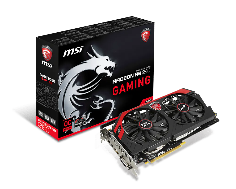
Radeon R9 280 GAMING 3G
AMD Radeon™ R9 280
PCI Express x16 3.0
933MHz Core (Boost Clock:1000MHz) (OC mode)
933MHz Core (Boost Clock:972MHz) (Gaming mode)
933MHz Core (Boost Clock:933MHz) (Silent mode)
933MHz Core (Boost Clock:972MHz) (Gaming mode)
933MHz Core (Boost Clock:933MHz) (Silent mode)
5000
384 bits
250
1x6-Pin, 1x8-Pin
500
269x128x37 mm
849
12 API
4.3
Up to 6 displays with the use of a DP MST Hub
3072
GDDR5
CrossFireX
240
DL-DVI-I x1Max Resolution: 2560 x 1600 @60 Hz
1 (version 1.4a)
Max Resolution: 3840x2160 @30 Hz
4096x2160 @24 Hz
Max Resolution: 3840x2160 @30 Hz
4096x2160 @24 Hz
2(version 1.2)
Max Resolution: 4096x2160 @ 50 Hz
Max Resolution: 4096x2160 @ 50 Hz
400
© AMD, and the AMD Arrow logo, Radeon, FreeSync, and combinations thereof are trademarks of Advanced Micro Devices, Inc. DirectX and Microsoft are registered trademarks of Microsoft Corporation in the US and other jurisdictions. PCI Express is a registered trademark of PCI-SIG Corporation. Vulkan and the Vulkan logo are trademarks of the Khronos Group Inc. Other product names are for identification purposes only and may be trademarks of their respective companies.
HDMI™、HDMI™ High-Definition Multimedia Interface、HDMI™ 商業外觀及 HDMI™ 識別標章等詞彙均為 HDMI™ Licensing Administrator, Inc. 的商標或註冊商標。
產品規格與配備可能會隨地區而有所不同,本公司另保留變更規格不另行通知權利。購買前請與當地線上或實體通路經銷商確認產品規格。
‘Boost Clock Frequency’ is the maximum frequency achievable on the GPU running a bursty workload. Boost clock achievability, frequency, and sustainability will vary based on several factors, including but not limited to: thermal conditions and variation in applications and workloads. ‘Game Frequency’ is the expected GPU clock when running typical gaming applications, set to typical TGP (Total Graphics Power). Actual individual game clock results may vary. © 2021 Micro-Star Int'l Co.Ltd. MSI is a registered trademark of Micro-Star Int'l Co.Ltd. All rights reserved.
